If you can 3D print electronics and then integrate them into a 3D form, a wide range of new applications will arise. From sensors to lighting fixtures to panels with integrated lighting, all produced in one process. TNO, together with several partners in the 3DOP project, shows that the technology works. Now it’s for commercial parties to develop the applications.
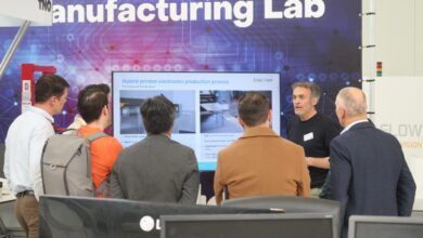
At Holst Centre on the High Tech Campus in Eindhoven, a joint venture of TNO and imec with 240 researchers are working on the technologies of tomorrow. Half of them do research for the semiconductor industry; the other half works on flexible and printed electronics, which traditionally have been a focus topic of TNO. The latter also has a link with the semiconductor industry, explains Hylke Akkerman, researcher and program manager. “We are trying to convert the thin-film deposition techniques that we have developed for OLED displays, among other things, to applications in the semiconductor industry, for example for chip packaging. Traditionally, this is done by applying a layer around the chips on the wafer. We do this on glass, which is more cost-effective.”
Researchers manage to print in a resolution of 20 microns; in one year, 10 microns should be achievable
3D printed electronics for large series
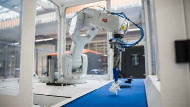
The team that Hylke Akkerman manages, works in parallel on 3D printed electronics, for example for wearables for health applications. Or on an ultrasound sensor that is integrated into the tip of a catheter. The technology developed for this in Eindhoven is based on resins. At the moment, the researchers manage to print in a resolution of 20 microns; in one year, 10 microns should be achievable. “And reproducible,” Akkerman emphasizes, because it is ultimately about the development of this production technology for large series.
Participation in 3DOP project
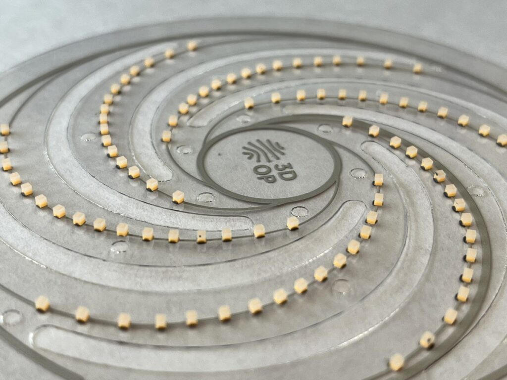
TNO is one of the partners in the 3DOP project. In Work Package 3 (3D Printed Molds & Electronics), TNO is working with partners to develop a solution for integrating thin-film printed electronics into a 3D form. Hylke Akkerman takes a piece of plastic foil on which all the silver strips are printed and topped with the LEDs. This is done with printing technology, where a lot of experience has already been developed at Holst Centre. In the 3DOP project, the challenge is to integrate these films into a 3D form, so that you get an end product in which the electronics are integrated.
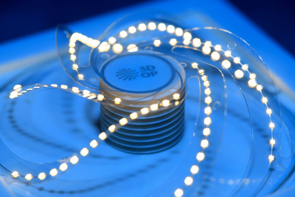
Japanese Kirigami
In a first step, the thin film – containing the electronics on top – is coated with plastic via injection moulding. Then the 3D object is formed. To do this, the researchers are reverting to an ancient Japanese art form: kirigami, a variant of origami. The material is now not only folded (as with origami) but also cut loose. Think of a greeting card that takes on a 3D shape when you unfold it. By cutting and folding the polymer part containing the electronics in the right places, you can create a 3D shape. This reduces the load on the electronics. Hylke Akkerman: “Normally, when you distort printed electronics, you start stretching and stretching. That has its limitations. Because the shape is now predefined, there is minimal elongation and the impact on the electronics is therefore small.”
Cheaper process
Hylke Akkerman estimates the TRL level at 6 or 7. The researchers have shown that the combination of printed electronics and kirigami can be used to create complex 3D shapes with integrated electronics. “Our technology is cheaper because we print the electronics in 2D. Otherwise, you need a pick and need to place a robot. And if you use thermoforming, you are limited by the restrictions that apply to this. The kirigami process allows us to use hard plastics to create complex 3D shapes.” According to the TNL researcher, applications include sensors in cars or stretchable displays.
Signify integrates the plastic parts containing the electronics into a luminaire
Three different demonstrators
Together with Tracxon and Signify in the Netherlands, and Tecos in Slovenia, TNO has built the first demonstrator within the 3DOP project: a lamp. Tecos has 3D printed metal molds for the overmolding of the electronics. Signify integrates the plastic parts containing the electronics into a luminaire. A second demonstrator is a ceiling panel for a motorhome in which the lighting is integrated. This is being developed together with the Centre for Applicable Polymers (CAP) in Slovenia. These two concepts will be further developed into prototypes in the coming months. A third demonstrator is a temperature sensor on flexible plastic film integrated into a metal mold. “You can measure the temperature of the mold during injection molding, which gives you better process control. Tecos has now shown that this works,” says Akkerman.

Step forward
The research institute conducts research at a relatively low TRL level and develops new concepts; the industry must then get to work on this. “We have to see how kirigami electronics lands with the industry. It should become a tool in their toolbox,” says the researcher. He himself wants to continue to take 3D printed microelectronics to a higher TRL level. This could offer even more possibilities in the long run.
For TNO, most of the work in the 3DOP project is done. Hylke Akkerman looks back with satisfaction. “This project has helped us move forward. We have taken a step forward by showing that you can integrate 3D printed electronics into hard plastics with complex shapes.” A next step could be to automate the various steps in the current process. The European project has also brought Hylke and his team also into contact with other 3D fabrication techniques, for example for ceramics and metal. “We can potentially do something with that.”